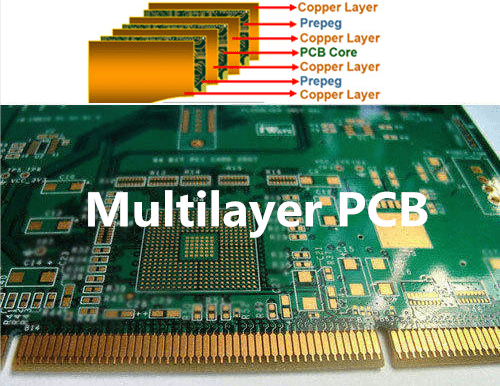
Multilayer PCBs have multiple layers connected with plated through holes and vias. Technology advancement has increased the demand for such PCBs in the market that are complex to handle due to various reasons. Especially for high voltage PCB design considerations, it should be as reasonable as possible to make the manufacturing process go more smoothly. This article discusses multilayered PCB manufacturing in detail before outlining the restrictions to ensure qualitative performance.
Multilayered PCB manufacturing stages
Following are the steps to manufacturing PCB after designing its prototype FS Tech.
Initial design printing
The PCB manufacturers print the PCB design or the images on the transparent film. They press the plated through holes drilled on the board to locate the placement of the components.
Structure with coper
They also print the inner part of the PCB design. They do so by applying the copper to the covered layers of the PCB to consider its structure.
Removal of copper residues
The manufacturers then remove the copper from the board that has to loosen its photosensitive power to sustain the etchant’s attack. This photoresist-free copper is unwanted, so they dispose of it. The manufacturers then cover the multiple layers of the PCB after layering them.
Drilling diameter holes
The manufacturers drill holes on the board using X-ray appliances. It helps to keep the pile of the layers in place while drilling required diameter holes.
Copper and Tin electroplating
After spreading a light layer of chemicals to merge the layers, the manufacturers electroplate the PCB with copper. They apply a photoresist on the copper plating done at the outer layers to increase its durability. The tin plating further secures the multilayered PCB.
Remove copper for traces and pads
The manufacturers do the tin plating to protect the required copper layer. They remove the unwanted and free photoresist copper plating to establish the electrical connections on the clean PCB by drawing signal traces and rout tabs.
PCB soldering
The manufacturers do the PCB soldering by applying epoxy solder mask ink on the board and exposing it to ultraviolet light. They then pass the board through the oven to firmly fix the solder mask. Gold and silver electroplating secure the PCB, followed by the ink-jet silkscreen writing application.
PCB testing
The manufacturers conduct multiple testing of the PCB to check its working and performance after welding the PCB components and securing the board.
Profiling and board cutting
They disconnect the PCBs from the panel after ensuring their optimum working and deliver it after reviewing the possible flaws on the board.
Limitations in its manufacturing
Mechanical and electrical challenges
The mechanical and electrical challenges are common during PCB manufacturing, like bows, twists, element mounting, etc. The fabricators can rectify these by using accurate parameters and suitable material and components for the PCB.
Rupturing of the PCB layers
OCB layers get delineated if the layers exceed the maximum level due to distortion in the copper layers. This limitation generally calls for spinning the board again to fix it.
Vias issues
The manufacturers generally face the challenge of choosing the via type for the PCB. They find it difficult to decide between blind or buried vias. Moreover, the drilling holes for these vias are also challenging in multilayered PCBs.
Heat generation and short circuit
The PCB components generate heat during the process. So, the multilayered PCBs require insulation to evade short circuits due to excessive heat. FR4 material is preferable for insulation between layers or the material whose hygroscopic level is low to avoid moisture.
Conclusion:
Multilayered PCBs are comparatively lightweight, compact, robust, and have greater assembly dimensions than single-layer PCBs. However, its manufacturing is challenging because of several hurdles that directly influence the PCBs functionality. Therefore, the manufacturers should comprehensively understand the limitations and follow the steps discussed above for qualitative and efficient PCB manufacturing.


![Anso FG Reviews: UPDATED 2024 [ansofg.com] Anso FG Reviews UPDATED 2024 [ansofg.com]](/wp-content/uploads/2023/12/Anso-FG-Reviews-UPDATED-2024-ansofg.com_-100x70.png)


